Source
Adapted from my own handwritten and hand-typed notes from Year 1 to Year 3 of my EEE degree
With one transistor there are three useful ways to choose the input and output terminals. The third terminal is at AC ground (through a bypass capacitor or a supply). All of them use the same four-resistor bias; only the coupling and bypass capacitors change.
Families
| Family | BJT | MOSFET | Character |
|---|---|---|---|
| Inverting amplifier | C-E: in at B, out at C | C-S: in at G, out at D | high gain, inverting |
| Voltage follower | C-C: in at B, out at E | C-D: in at G, out at S | gain close to 1, high , low |
| Non-inverting amplifier | C-B: in at E, out at C | C-G: in at S, out at D | gain , low |
General Analysis Pattern
Quantities:
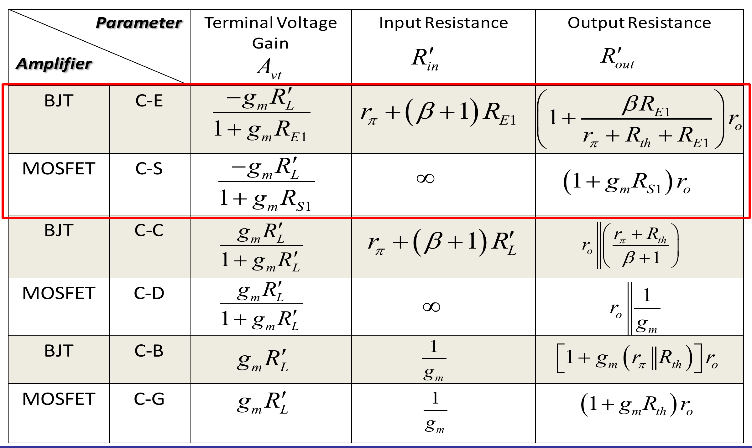
- terminal gain from the transistor input terminal to the output
- input resistance including the bias resistors, which forms a divider with the source resistance
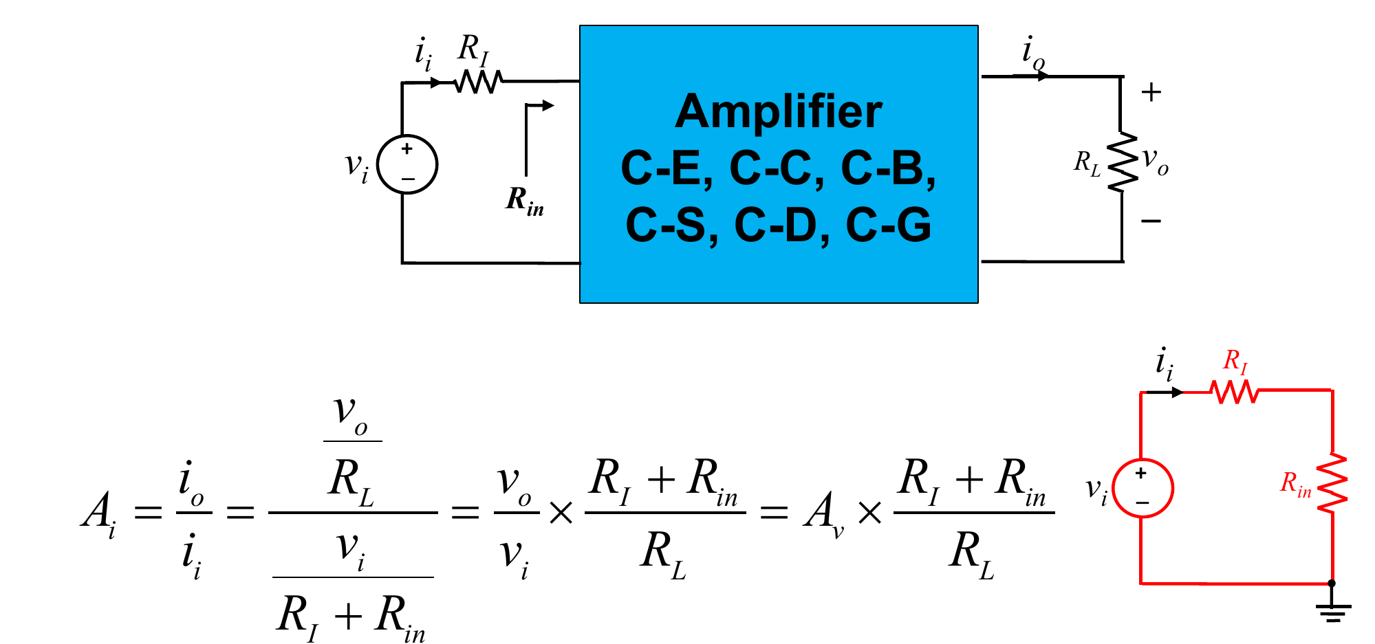
- overall gain
- output resistance found by killing and applying a test source at the output
Primed values (, ) are looking into the transistor terminal only, before the bias resistors are put in parallel.
Summary Table
Current Gain
So a follower, with gain near 1 but large , can still give a large current gain.
The buffer family is worked out in Common-Collector and Common-Drain Followers.