Source
Adapted from my own handwritten and hand-typed notes from Year 1 to Year 3 of my EEE degree
Clock Signal
A clock is a periodic square wave that tells synchronous circuits when they may change state.
Clocked SR Flip-Flop
Two NAND gates in front of a cross-coupled NAND cell gate and with the clock. When both gate outputs are 1, so the cell rests. When , and act like active-high set and reset.
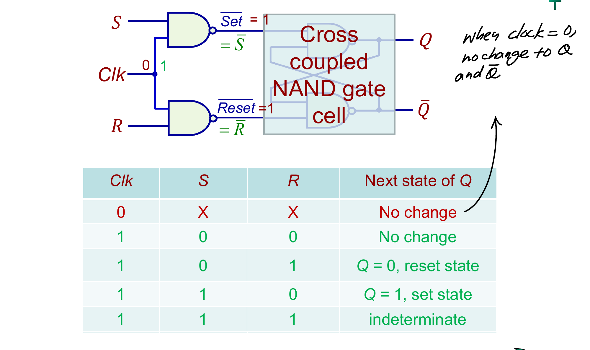
Characteristic Table and Equation
The characteristic table gives the next state from the inputs and the present state . The characteristic equation is the minimised form from a K-map. For the SR flip-flop (with as a don't-care):
Including an active-high clock: .
Excitation Table
The excitation table is the reverse: for a wanted transition it lists the inputs needed. It is the main tool for designing counters and state machines.
Four Flip-Flop Types
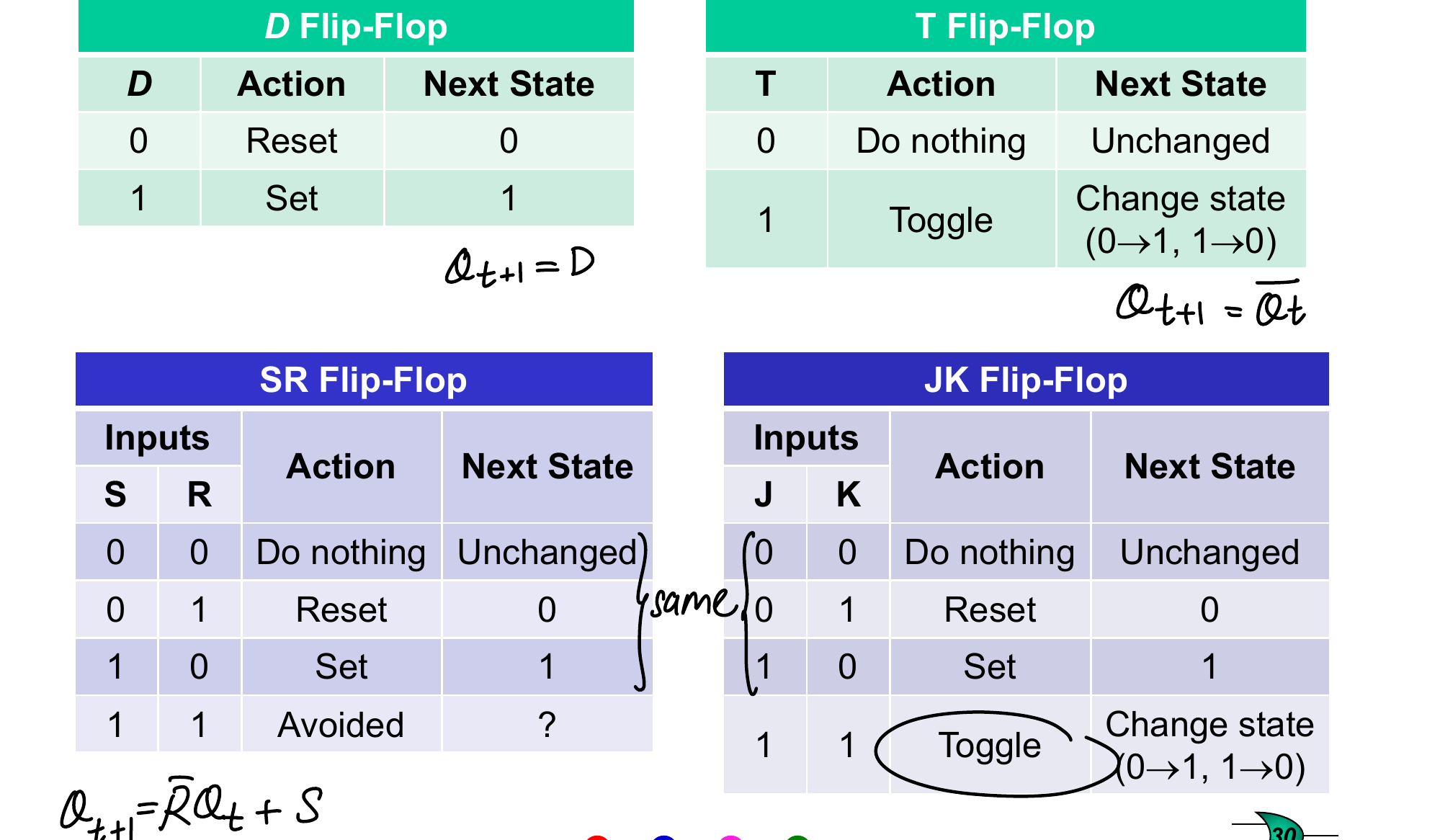
| Type | Behaviour | Characteristic equation |
|---|---|---|
| SR | set, reset, hold, not allowed | |
| D | output follows | |
| JK | like SR, but toggles | |
| T | toggles, holds |
Excitation tables (x is a don't-care):
| 0 to 0 | 0 | x | 0 | x | 0 | 0 |
| 0 to 1 | 1 | 0 | 1 | x | 1 | 1 |
| 1 to 0 | 0 | 1 | x | 1 | 0 | 1 |
| 1 to 1 | x | 0 | x | 0 | 1 | 0 |
Building D, JK and T From SR
Every flip-flop is a basic cell plus input forming logic (IFL), which decodes the inputs, clock and present state into set/reset signals and never asserts both together.
Constructions:
- D: from the SR excitation table, and , so one inverter is added. When the clock is asserted follows , otherwise it is latched
- JK: acts as set and as reset, with and fed back to the input NAND gates so that toggles instead of being forbidden
- T: a JK flip-flop with and tied together as
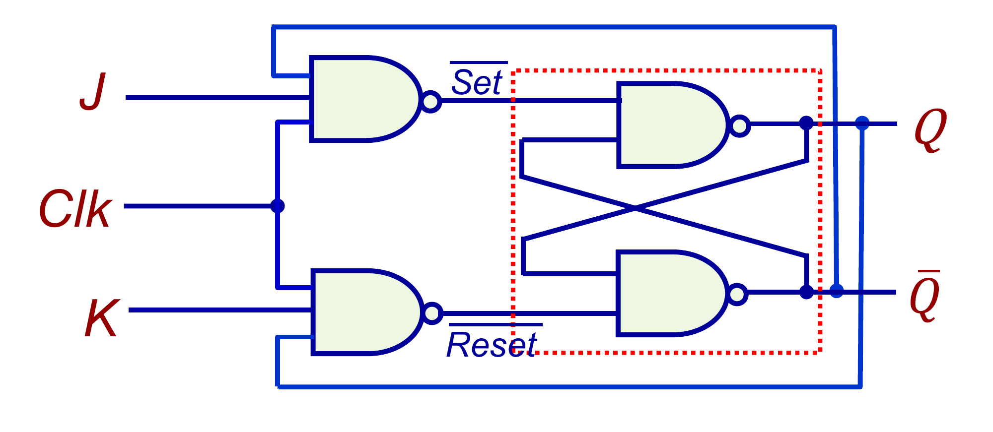
With a level-sensitive clock, a JK in toggle mode keeps toggling as long as the clock is high. This race problem is why proper Flip-Flop Triggering Schemes are needed.