Source
Adapted from my own handwritten and hand-typed notes from Year 1 to Year 3 of my EEE degree
Types of RAM
RAM types:
- SRAM (static): each cell behaves like a latch and keeps its value as long as power is on
- DRAM (dynamic): each cell holds charge for only a few milliseconds and must be refreshed
- NVRAM: RAM plus a battery, so it is non-volatile
SRAM Cell
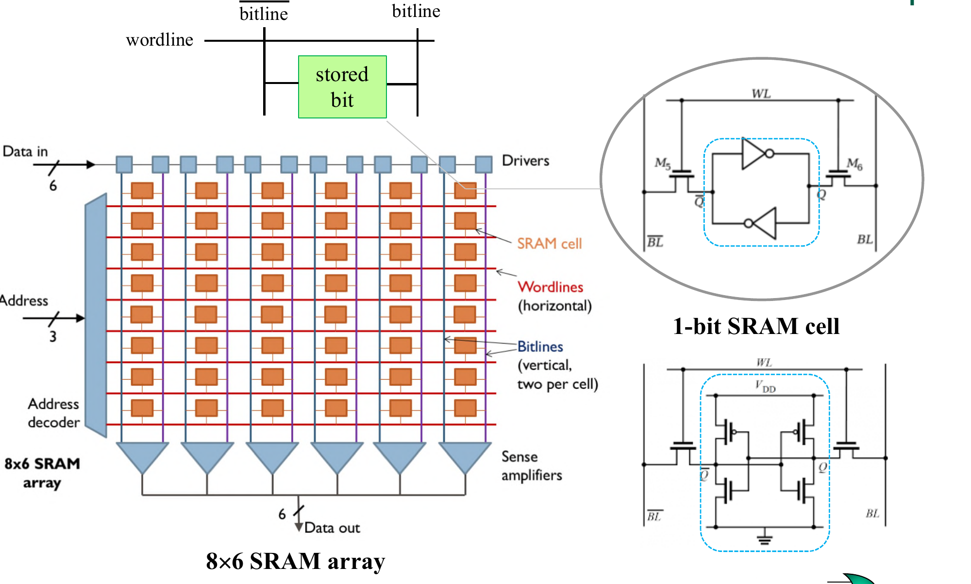
A 1-bit SRAM cell is two cross-coupled inverters (a bistable latch) plus two access transistors, six transistors in total. The wordline turns on the access transistors and connects the cell to a complementary pair of bitlines, bitline and . Sense amplifiers at the bottom of each column read the small difference between the two bitlines.
Control Lines
Controls (usually active low):
- : write enable
- : chip select
- : output enable
Many SRAMs use bidirectional data pins: the same pins carry data in for a write and data out for a read, using tri-state buffers. This suits wide devices and bidirectional microprocessor buses.
Read Timing
SRAM read timing is the same as ROM read timing (, , , , ) with held HIGH.
Write Timing
A write happens while both and are low, either WE-controlled or CS-controlled. Rules:
- the address must be stable before the write starts and after it ends
- the data is latched on the trailing edge of the write pulse ( and both low)
Parameters:
- : address setup before the write
- : address hold after the write
- : chip select setup before the end of the write
- : minimum write pulse width
- : data setup before the end of the write
- : data hold after the end of the write
These play the same role as setup and hold for a flip-flop. The denser but slower alternative is DRAM Operation and Refresh.