Source
Adapted from my own handwritten and hand-typed notes from Year 1 to Year 3 of my EEE degree
DRAM Cell
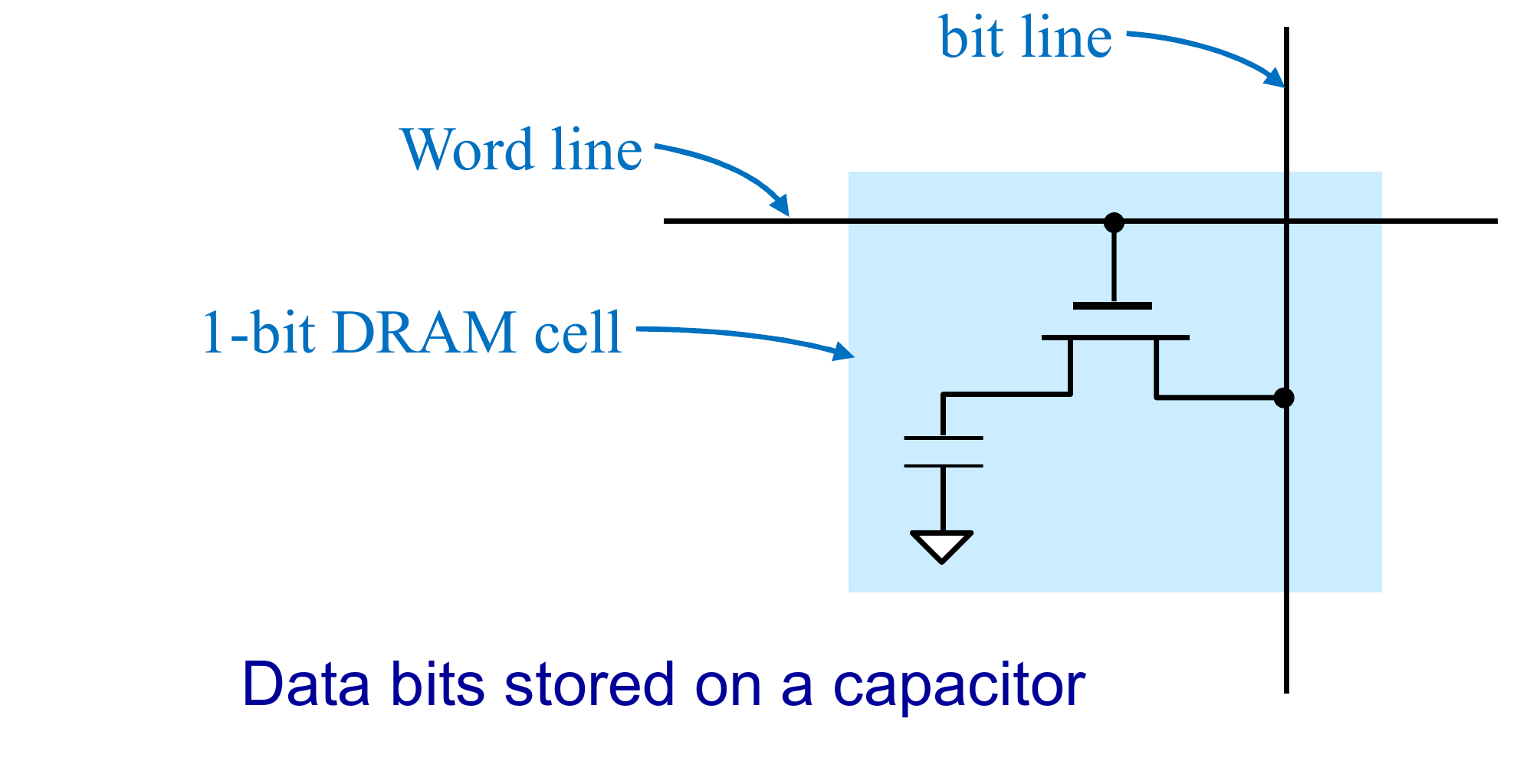
A DRAM cell is one transistor and one capacitor (1T1C), compared with six transistors per bit in SRAM. A charged capacitor is a 1, a discharged one is a 0. It is called dynamic because the charge leaks away, so the value must be rewritten periodically and after every read. DRAM was invented by Robert Dennard at IBM in 1966.
| SRAM | DRAM | |
|---|---|---|
| Transistors per bit | 6 | 1 (plus a capacitor) |
| Cell size and cost | larger, higher | smaller, lower |
| Power | higher | lower |
| Speed | faster | slower |
| Refresh | not needed | needed |
Read
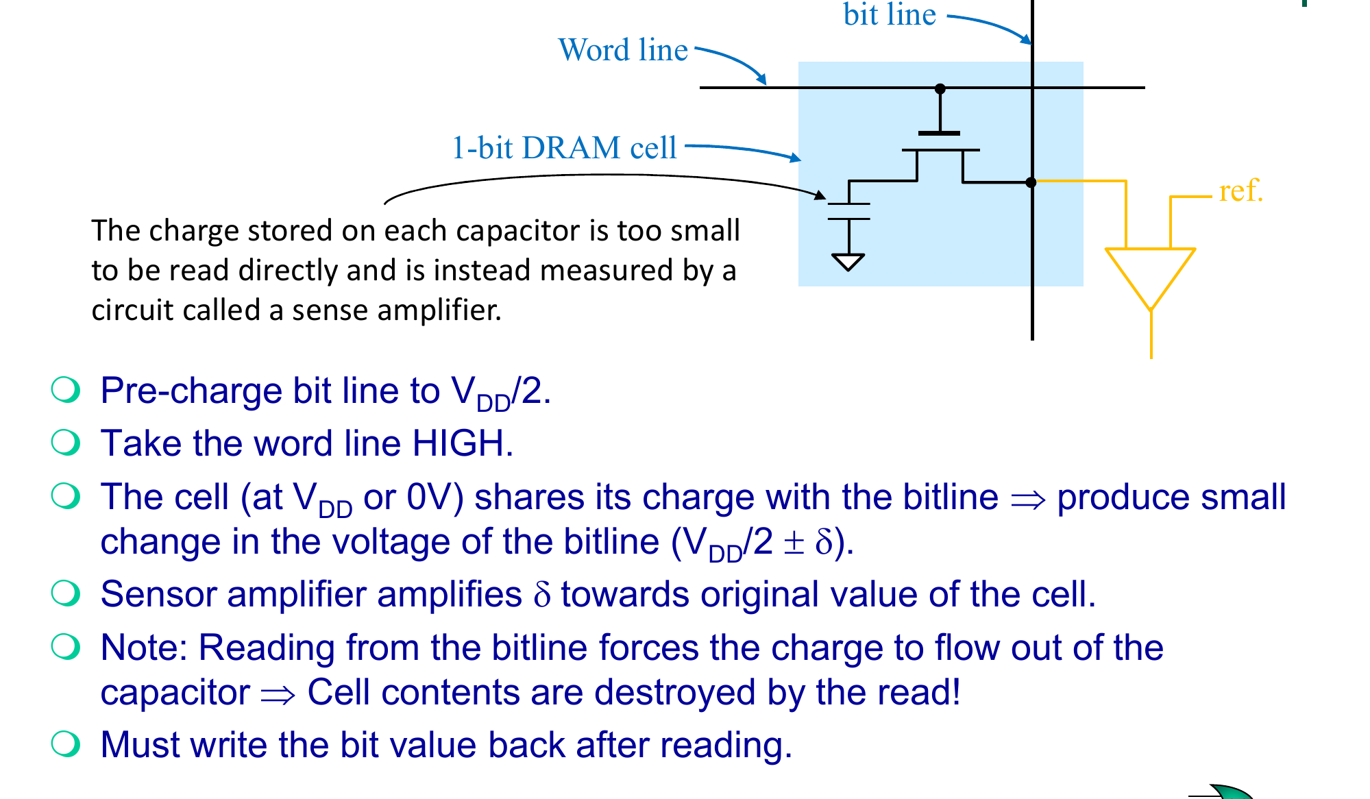
The stored charge is too small to read directly, so a sense amplifier is used:
- pre-charge the bitline to
- take the wordline HIGH
- the cell shares its charge with the bitline, moving it slightly to
- the sense amplifier amplifies back to a full logic level
Reading drains the capacitor, so the read is destructive and the value must be written back after every read.
Write
Steps:
- take the wordline HIGH
- drive the bitline LOW to store a 0 or HIGH to store a 1
- take the wordline LOW to isolate the capacitor
A stored 1 leaks away as . The refresh period is the time for to fall from to the minimum voltage that still reads as a 1.
Internal Organization and RAS/CAS
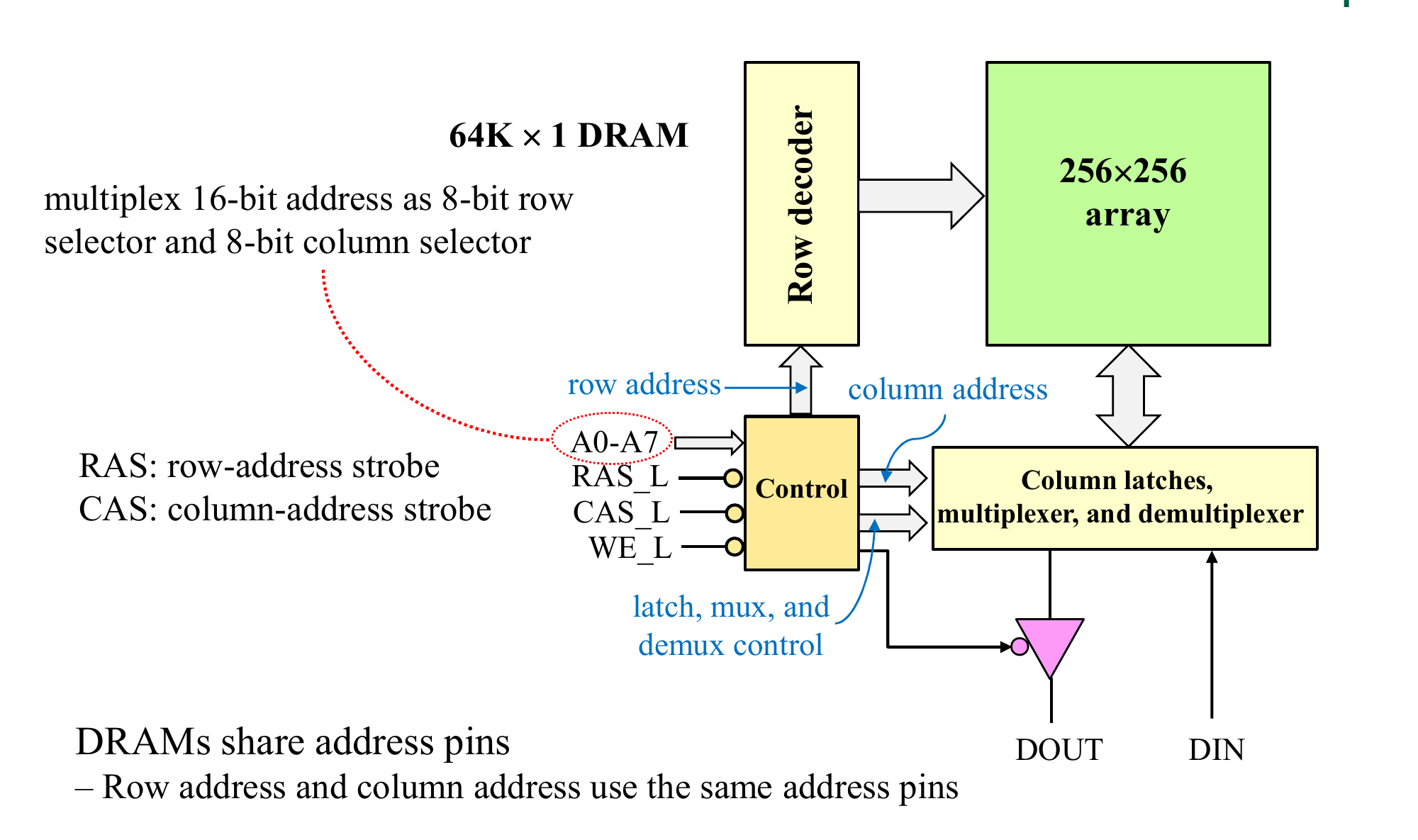
To save pins, DRAMs multiplex the address: the row address and column address share the same pins.
How it works:
- address bits are given in two halves on pins
- on the falling edge of (row address strobe) the row address is latched and the whole row is read into the row latch
- on the falling edge of (column address strobe) the column address is latched and one bit is selected for output (or merged with for a write)
- for a write, must be asserted before
Example: a 64K x 1 DRAM is a 256 x 256 array with 8 address pins; a 1M x 1 DRAM () has 10 address pins. Older DRAMs are asynchronous; modern SDRAM uses a clocked interface.
Refresh
Each cell typically needs a refresh every 4 to 64 ms. A RAS-only refresh cycle applies a row address and pulses , which reads the row and writes it back without any data at the pins. Refresh takes roughly 1% of DRAM cycles.
The refresh circuitry is a refresh counter holding the next row address plus a timer that steps it. Refresh can be burst (all rows at once) or distributed (spread evenly).
Example: 64 ms refresh interval and 8,192 rows gives a refresh cycle every .
Larger memories have higher refresh overhead, so each chip is divided into banks that are refreshed in parallel.