Source
Adapted from my own handwritten and hand-typed notes from Year 1 to Year 3 of my EEE degree
Memory Array
A memory is a 2D array of bit cells, each storing one bit. With address bits and data bits:
- depth rows (number of words)
- width columns (word size)
- array size bits
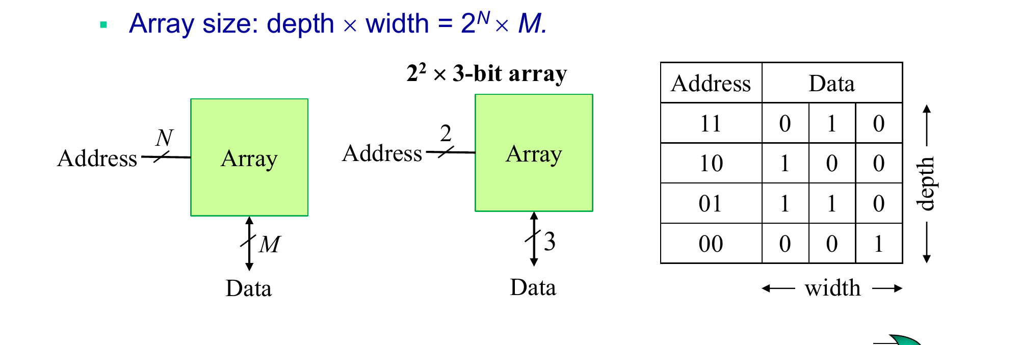
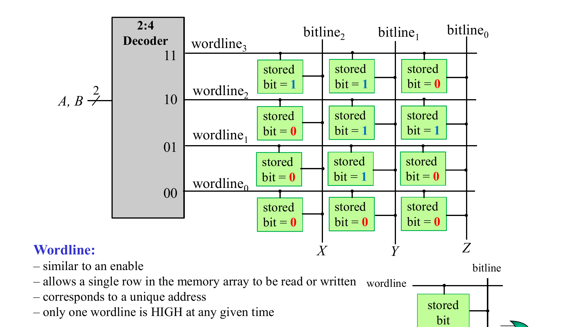
A wordline is like an enable: the address decoder drives exactly one wordline HIGH, selecting one row to read or write. Bitlines carry the data of each column.
ROM vs RAM
| ROM | RAM | |
|---|---|---|
| Volatile | no, keeps data without power | yes, loses data without power |
| Read | fast | fast |
| Write | impossible or slow | fast |
| Examples | boot ROM, firmware, flash in cameras and phones | main memory |
The names are historical: ROMs were once written at manufacture or by blowing fuses, and "random access" means any word is as easy to reach as any other, unlike a magnetic tape.
Logic With a ROM
A ROM is a lookup table, so it can implement any combinational function: the inputs are the address and each output bit is a column.
Example: , , in a -bit ROM:
| 00 | 0 | 0 | 0 |
| 01 | 0 | 1 | 0 |
| 10 | 0 | 1 | 1 |
| 11 | 1 | 1 | 0 |
Two-Dimensional Decoding
A long thin array is impractical (a 1M x 1 RAM with one decoder would need 1,048,576 20-input NAND gates). Instead the array is kept roughly square:
- address bits drive a row decoder to pick one of rows
- each row holds words of bits
- the remaining address bits drive a column multiplexer that picks one -bit word from the row
Example: a 32K x 8 ROM ( words, so 15 address lines A0 to A14) built from eight 512 x 64 arrays. A6 to A14 go to a 9-to-512 row decoder and A0 to A5 select one of 64 columns in each array through 64-to-1 MUXes, one array per data bit D0 to D7.
ROM Control Signals and Timing
A ROM chip has address inputs, data outputs and two active-low controls: chip select and output enable . Outputs are tri-state.
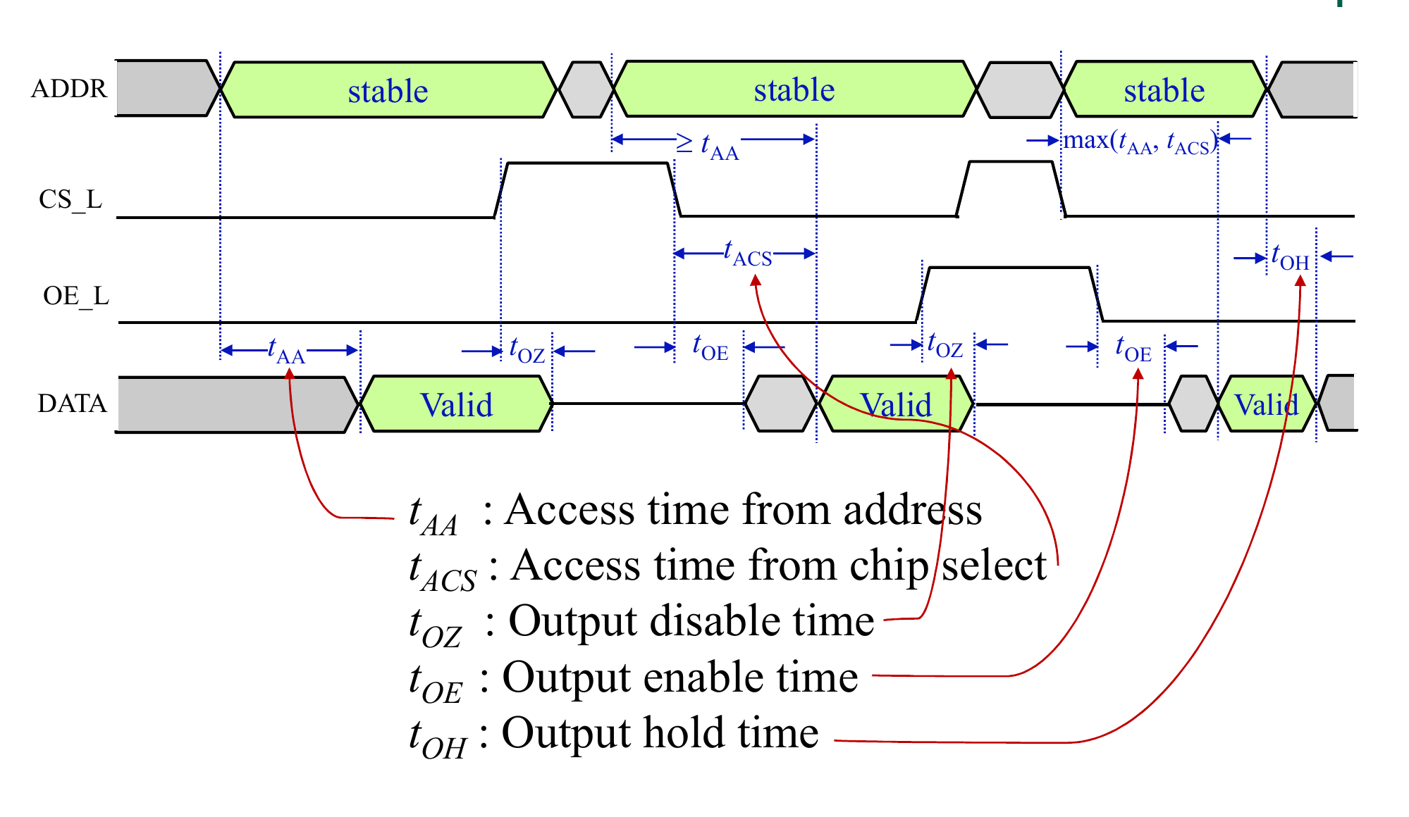
Timing parameters:
- : access time from address
- : access time from chip select
- : output enable time
- : output disable time
- : output hold time after the address changes
Data is valid after , provided has also been low for .