Source
Adapted from my own handwritten and hand-typed notes from Year 1 to Year 3 of my EEE degree
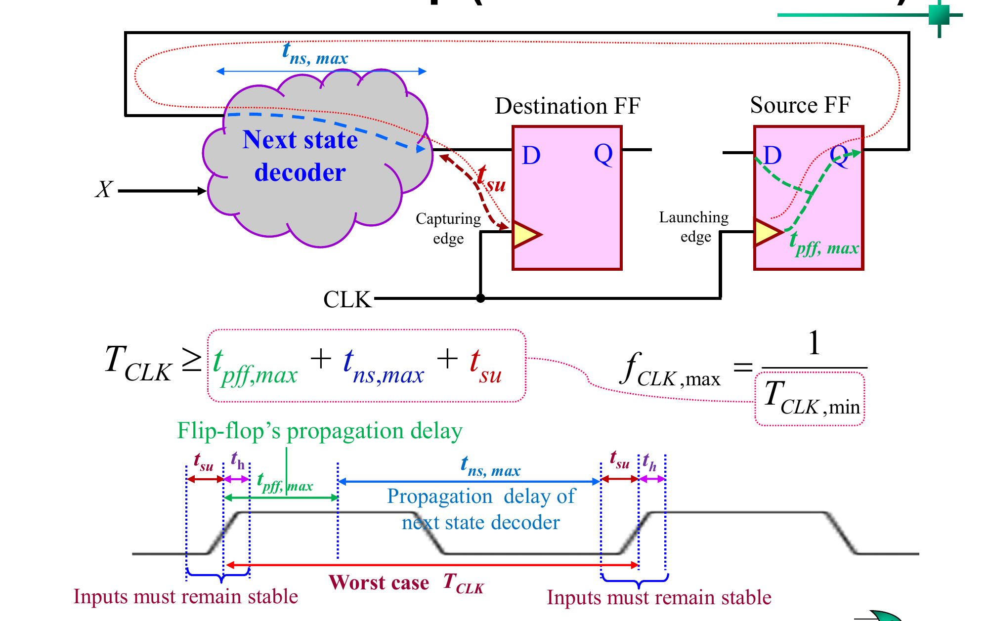
Minimum Clock Period
Data launched at one clock edge must pass through the flip-flop, through the next-state decoder, and settle a setup time before the next edge:
where is the flip-flop clock-to-output delay and is the worst-case delay of the next-state decoder.
Example 1: Inverter Feedback
A D flip-flop with its output fed back through an inverter. Data: ns, ns, ns, ns, ns.
Setup check (slowest path):
Hold check (fastest path):
No violation. With ns the hold margin is still 10 ns, but ns, so there is a setup violation. Here ns, so MHz.
Example 2: Two Flip-Flops
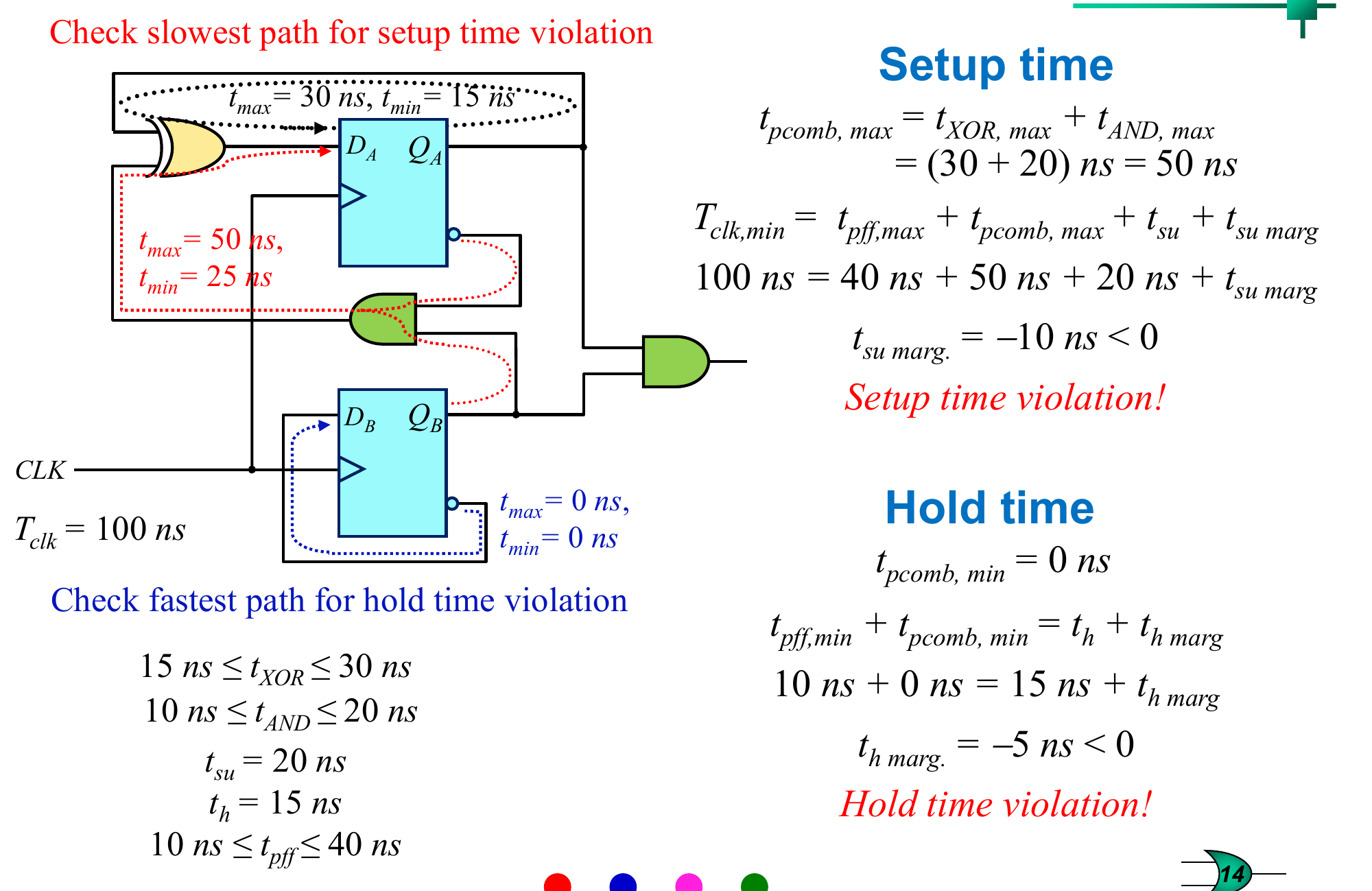
Data: ns, ns, ns, ns, ns, ns.
Setup, slowest path through XOR and AND:
Setup violation.
Hold, fastest path is the direct wire with :
Hold violation. Lowering the clock frequency fixes the setup problem but never the hold problem, which needs extra delay in the short path. See Setup and Hold Time for why.
Clock Uncertainty
The clock does not arrive perfectly at every flip-flop:
- clock skew: a fixed difference in arrival time of the same edge at different flip-flops, caused by wiring and buffers
- jitter: random cycle-to-cycle variation of the edge time
Both eat into the timing margins, so real designs keep a safety margin. In a shift register, if the destination flip-flop's clock arrives later than the source's by more than , the destination loads the new data instead of the old, which is a hold-type failure.